Scanning Near-field Microwave Microscopy
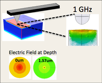
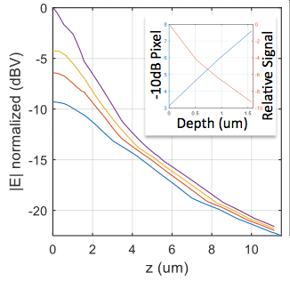
SNMM is a method for performing microwave characterization of materials and devices (e.g., permittivity, permeability, conductivity). In addition to material characterization, it is hoped that SNMM can be used to detect defects and trojans in fabricated integrated circuits. One particular target of interest is dopant concentrations because this is a critical measurement for device validation and becuase of the recent demonstration of dopant-level hardware trojans. The dopant lies below many microns of top-side (back-end-of-line) metal routing, or through several microns (up to 100's of microns) of back-side doped silicon. This is bad news for spatial resolution "at depth" because the nanometer spatial resolution of an SNMM is only possible in the near-field of a nanometric scannig tip. At micron depths spatial resolution has degraded by two orders of magnitude. We are examining methods for enhancing sub-surface spatial resolution by employing novel lock-in detection methods which enhance the signal response from only the target of interest (e.g., doped regions). We are examining quasi-static as well as highly dynamic mid-IR electromagnetic fields for the modulation of doped regions.